Original Link: https://www.anandtech.com/show/13786/snapdragon-855-performance-preview
The Snapdragon 855 Performance Preview: Setting the Stage for Flagship Android 2019
by Andrei Frumusanu on January 15, 2019 8:00 AM EST- Posted in
- Qualcomm
- Smartphones
- Mobile
- SoCs
- 7nm
- Snapdragon 855

As we get ever closer to the releases of various Android vendor’s newest generation devices, Qualcomm continues its tradition of showcasing the performance of its newest generation SoC ahead of time, giving us a preview and a glimpse of what to expect of the upcoming commercial devices. This year, the company has shuffled the schedule around a bit, and instead of hosting the event at their San Diego headquarters, and we were able to get a hands-on with the Snapdragon 855 at CES before the show had started. Today we’re be looking in quite extensive detail on how exactly the new Snapdragon chipset performs, as well as shedding some light on some important unanswered technical questions on some aspects of the SoC.
It’s been roughly a little over a month now since Qualcomm officially announced the Snapdragon 855 in Hawaii, and we had posted extensive coverage on the event and the various announcements that took place:
Full Coverage
Day One
- Qualcomm Tech Summit, Day 1 Live Blog (Starts at 2pm ET)
- Qualcomm Tech Summit, Day 1: Announcing 5G Partnerships and Snapdragon 855
- The Verizon and AT&T 5G Setups at Qualcomm’s Snapdragon Summit
- 5G Mobile Hotspots: Netgear for AT&T and inseego for Verizon
- A Quick Look at Qualcomm’s 5G Smartphone Reference Design
- Implementing 5G in the UK: EE Trial Sites and First Cities
- Samsung’s 5G Smartphone Prototype: Don’t Mention The Notch
- Moto 5G Mod at Snapdragon Summit: Lots of Antennas, and S855 Inside?
Day Two
- Qualcomm Tech Summit, Day 2 Live Blog (Starts at 2pm ET)
- Qualcomm Tech Summit, Day 2: Snapdragon 855 Mobile Platform
- The Qualcomm Snapdragon 855 Pre-Dive: Going Into Detail on 2019's Flagship Android SoC
- OnePlus: Dual Product Lines, Cost of 5G, and Translation Errors
- Snapdragon 855 Power Consumption Demo, But
- Snapdragon 855: 802.11ax-Ready / Wi-Fi 6 Demonstrations
Day Three
- Qualcomm Tech Summit, Day 3 Live Blog (Starts at 2pm ET)
- Spotted: Qualcomm Snapdragon 8cx Wafer on 7nm
- Qualcomm Tech Summit, Day 3: Snapdragon 8cx, the New ACPC SoC
For anyone who might have missed it, if there’s any one specific article that I would recommend reading before heading in directly to the results of the benchmarking session, then it’s our in-depth piece summarising the disclosed specifications of the new Snapdragon 855.
SoC Overview & CPU Recap
| Qualcomm Snapdragon Flagship SoCs 2018-2019 | |||
| SoC |
Snapdragon 855 |
Snapdragon 845 | |
| CPU | 1x Kryo 485 Gold (A76 derivative) @ 2.84GHz 1x512KB pL2 3x Kryo 485 Gold (A76 derivative) @ 2.42GHz 3x256KB pL2 4x Kryo 485 Silver (A55 derivative) @ 1.80GHz 4x128KB pL2 2MB sL3 |
4x Kryo 385 Gold (A75 derivative) @ 2.8GHz 4x256KB pL2 4x Kryo 385 Silver (A55 derivative) @ 1.80GHz 4x128KB pL2 2MB sL3 |
|
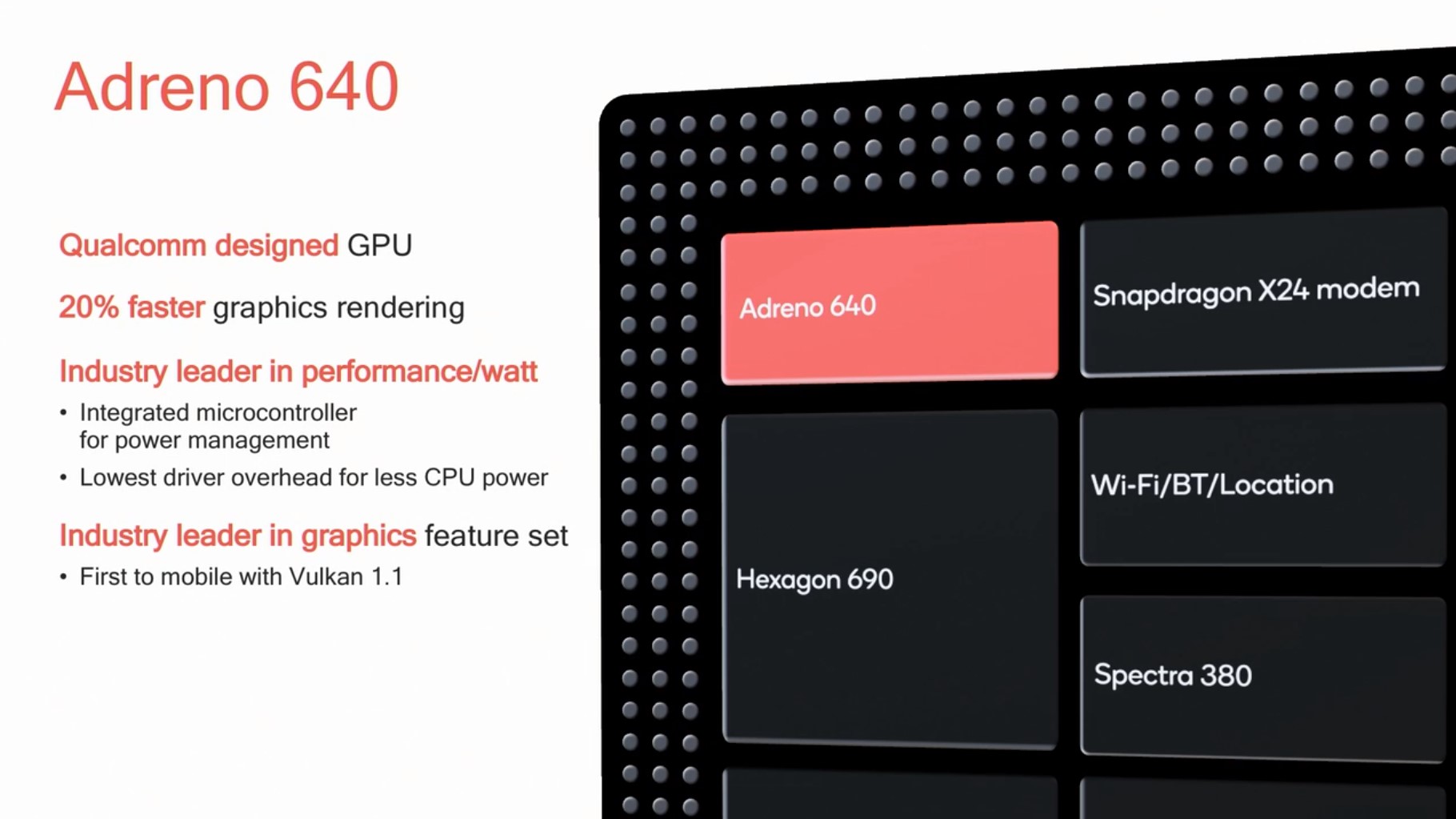
| GPU | Adreno 640 @ ?MHz | Adreno 630 @ 710MHz | |
| Memory | 4x 16-bit CH @ 2133MHz LPDDR4x 34.1GB/s 3MB system level cache |
4x 16-bit CH @ 1866MHz LPDDR4x 29.9GB/s 3MB system level cache |
|
| ISP/Camera | Dual 14-bit Spectra 380 ISP 1x 48MP or 2x 22MP |
Dual 14-bit Spectra 280 ISP 1x 32MP or 2x 16MP |
|
| Encode/ Decode |
2160p60 10-bit H.265 HDR10, HDR10+, HLG 720p480 |
2160p60 10-bit H.265 720p480 |
|
| Integrated Modem | Snapdragon X24 LTE (Category 20) DL = 2000Mbps 7x20MHz CA, 256-QAM, 4x4 UL = 316Mbps 3x20MHz CA, 256-QAM |
Snapdragon X20 LTE (Category 18/13) DL = 1200Mbps 5x20MHz CA, 256-QAM, 4x4 UL = 150Mbps 2x20MHz CA, 64-QAM |
|
| Mfc. Process | 7nm (N7) | 10nm LPP | |
Summarising the Snapdragon 855 quickly, at the heart of the new 7nm chipset we find four new Kryo 485 CPUs based on Arm’s new Cortex A76 cores. The new CPU cores are derivatives of the designs Arm makes available by default: Here Qualcomm takes advantage of the “Built on Arm Cortex Technology” license which allows vendors to demand changes to the IP based on a set of microarchitectural tuneables that Arm makes available. Even though the Snapdragon 855’s Kryo 485 is the third generation of such a derivative core from Qualcomm, it represents the first instance of the company actually talking about what kind of microarchitectural changes have been made to the CPUs. The Kryo 485 Cortex A76 derivatives increase the re-order buffer from Arm’s default 128 entries to a higher, undisclosed figure. Qualcomm has also revealed that the prefetchers have been optimised for better efficiency, although again we don’t have any details on how exactly this has been achieved. Finally, as I’ve understood it, the branch data structures have also seen an improvement over the default A76 configuration.

Although the SoC still comes in a “4+4” big.LITTLE high-level core configuration, the big cores in the S855 aren’t actually all equal: Here Qualcomm has gone for a rather exotic 1+3+4 configuration, in which one of the big cores is implemented with a higher frequency physical design reaching 2857MHz, all while also employing a larger L2 cache of 512KB. The remaining three big cores max out at 2439MHz and are only equipped with 256KB L2 caches. Qualcomm does clock this 1+3 configuration differently with asynchronous clock planes, however the cores still share the same voltage plane. Here the company explains that this is a compromise between power efficiency benefits, and cost of implementation complexity as well as supporting power delivery components (Adding an extra voltage plane adds another PMIC rail with inductors & capacitors).
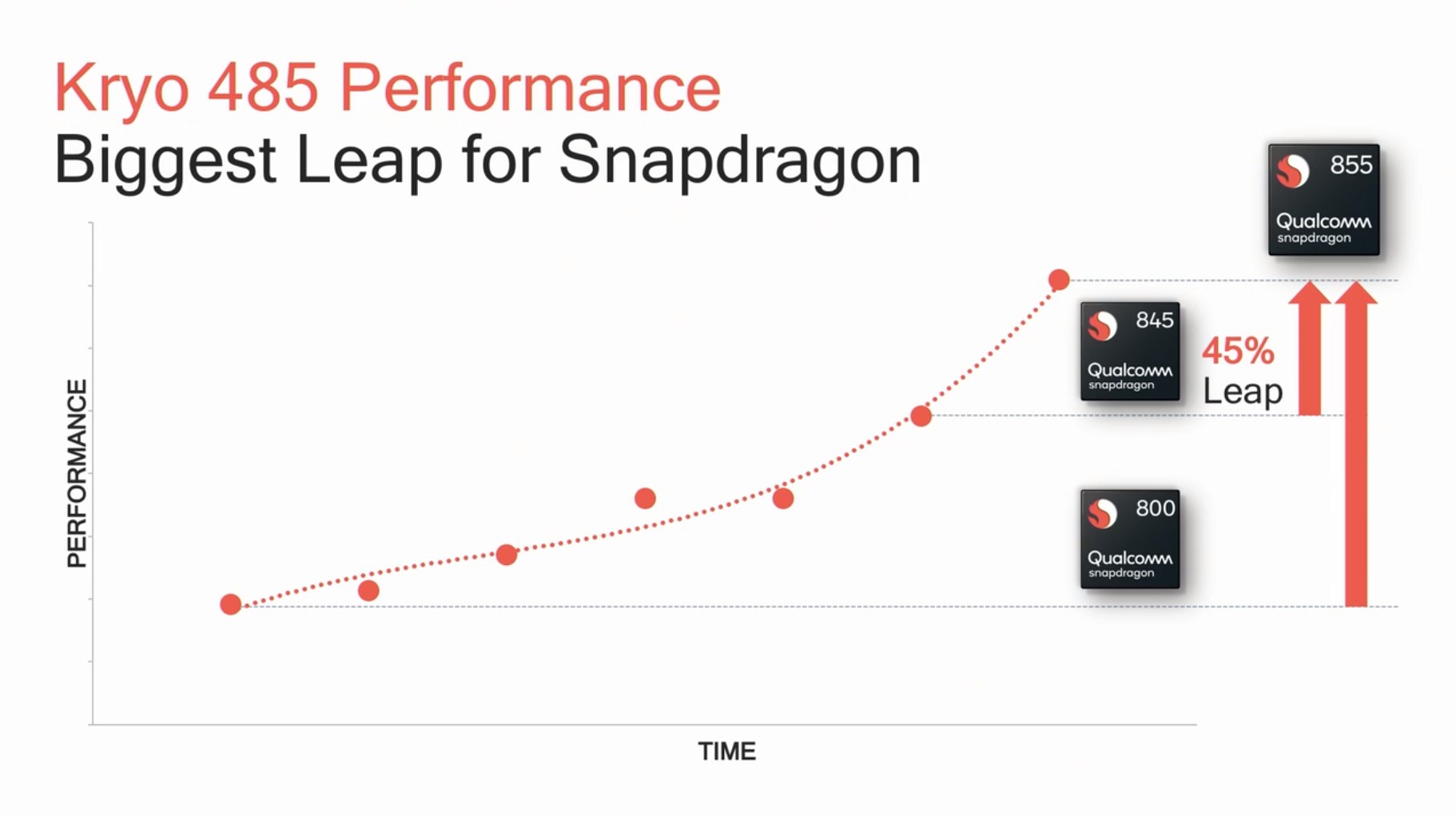
The Kryo 485 in the S855 promises to be Qualcomm’s biggest performance jump ever, advertising a 45% jump in performance compared to the Snapdragon 845. As we had discussed it in our launch article, this figure seems to coincide with the performance jump the Kirin 980 saw over the Snapdragon 845, which makes sense given that the two new SoCs both employ the newest generation A76 CPU at similar clocks.
The Snapdragon 855 QRD

Today’s testing platform is Qualcomm’s new Snapdragon 855 QRD (Qualcomm Reference Design). This year’s QRD design is probably Qualcomm’s most “commercial-device-like” ever as other than the more robustly built bezels, you would have a hard time noticing that this a reference platform – at least on the hardware side. The company stated that the QRD as tested should be a near representation of what to expect of commercial device – but of course vendors might still diverge from this as they may change the underlying software.
We’ve had a limited hands-on time with the devices, and although we managed to do a lot with them, some of the more time-intensive testing such as GPU sustained performance testing were out of the scope of today’s session.
The Big Question For The Snapdragon 855 : Memory Latency
One of the more odd developments that Qualcomm introduced with the Snapdragon 845 last year was the addition of a new 3MB system level cache that sits in front of the memory controllers as a new cache hierarchy. This new block is meant to serve as a SoC-wide buffer for the various IP blocks, reducing the amount of expensive DRAM memory accesses and thus improving power efficiency of the system. As well as improving power efficiency, it could in theory also serve as a booster for performance. The most famous use of such a system cache is Apple’s own A-series chips where we’ve seen this kind of IP block used ever since the A7.
Qualcomm’s introduction of such an IP block in the Snapdragon 845 was exciting to see, however this came as a double-edged sword as it had also introduced a 30% regression (In comparison to the Snapdragon 835) in DRAM memory latency, which may have limited some of the performance aspects of the A75-based CPU last year.
The new Snapdragon 855 unfortunately doesn’t seem to have made any major improvements in this regard as Qualcomm had confirmed that the IP block is the same as the one used in the Snapdragon 845.
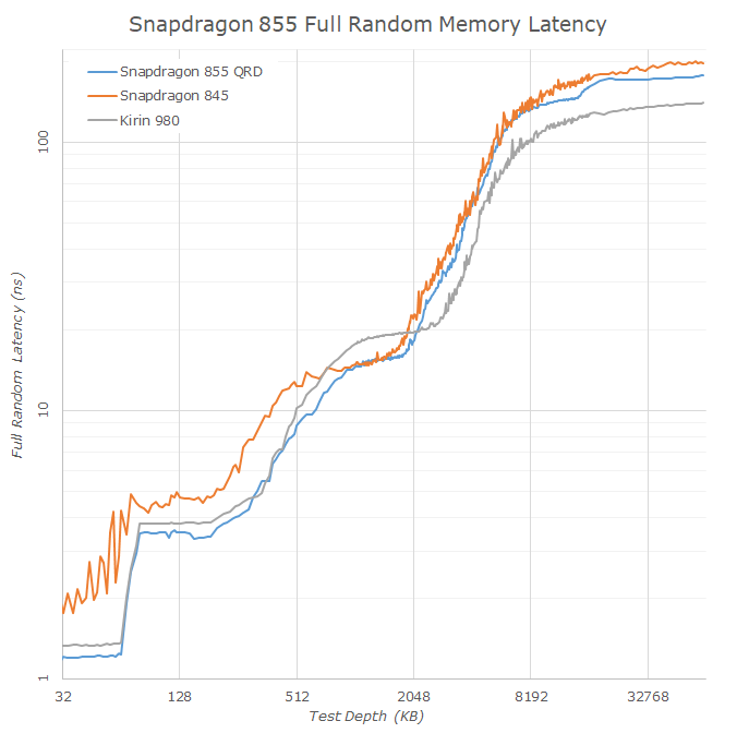
To investigate the differences between the Snapdragon 845, 855 and also the Kirin 980, we make use of latency test. First off, let’s view the memory hierarchy in a logarithmic latency graph, better visualising the various latency jumps between hierarchies:
Between the Snapdragon 845 and the new 855, we now see the increased L2 cache of the Kryo 485 Prime core at 512KB, an increase over the 256KB size on the previous generation performance core. What is also visible is that the L2 latency has improved, even though both chipsets are clocked near to each other at ~2.8GHz.
The DSU L3 cache on both the Snapdragon 845 and 855 are identical at 2MB in size: Again what’s interesting here to see is that the latency on this part of the cache hierarchy seems to be identical between both SoCs. This is in contrast to the 4MB L3 of the Kirin 980 which, albeit bigger, seems to be 20% slower.
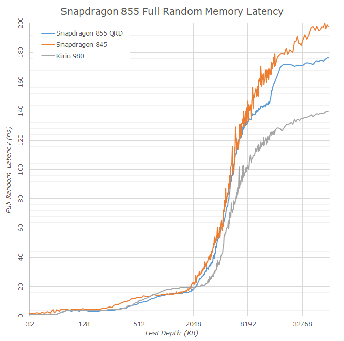
Moving onto the linear graph, here we can see the difference in DRAM latency in a clearer fashion. The Snapdragon 855 does seem to slightly improve memory latency over the 845, however this might just be an effect of the newer 2133MHz LPDDR4X memory that represents a 14% speed boost over the 1866MHz memory of last year’s devices.
Critically though, is the comparison to the Kirin 980 which employs the same CPU microarchitecture, and the same 2133MHz memory as the Snapdragon 855. Here Qualcomm still shows a notable latency regression in memory latency over the competition, whose effects will be interesting to analyse in the following pages.
CPU Performance & Efficiency: SPEC2006
We move on with our analysis by using SPEC2006 on the Snapdragon 855 QRD. SPEC2006 is an important benchmark as not only does it represent a tool that is used by many companies to architect their CPU designs, but it also a very well understood and academically documented workloads that can serve as a macro-benchmark to determine microarchitectural aspects of a CPU and system.
It’s to be noted that SPEC2006 has been deprecated in favour of SPEC2017, and although we’ll switch to that at some point, for mobile platforms SPEC2006 still represents a good benchmark. Because our scores aren’t official submissions, as per SPEC guidelines we have to declare them as internal estimates from our part.
A Big Note on Power on the QRD
Although for this article I was able to collect power figures for both CPU and GPU workloads, the figures are not of an as high certitude as when measured on commercial devices. The reason for this is that much like last year’s Snapdragon 845 QRD, this year’s 855 platform reports rather high idle power in the 950-1050mW range, about 500mW more than one would expect in a final product. Because our power measurement methodology represents publishing active system power, meaning we measure total power during a given workload and subtract the idle power under the same conditions, there is a degree of uncertainty if the idle power by default is quite high.
Today’s power efficiency figures thus merely represent a guideline – and we’ll make sure to re-test the results once we get our hands on final commercial devices.
The Results – The Snapdragon 855 Performs Admirably
We’ll start off with the aggregate results and drill down in the detailed results later:
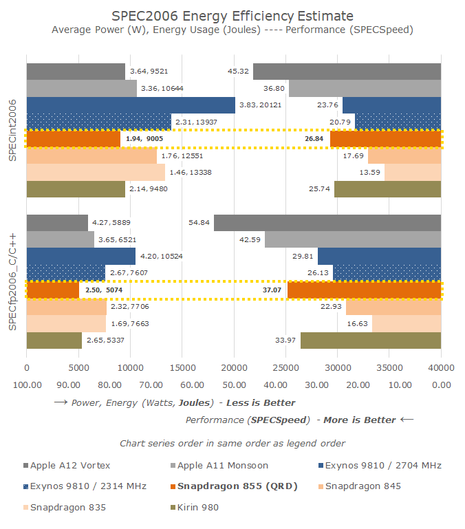
The Snapdragon 855 ends up performing extremely well, ending up neck-and-neck with the Kirin 980’s performance, which shouldn’t come as too big of a surprise.
In SPECint2006, the Snapdragon 855 performs 51% better than the Snapdragon 845, all while improving power efficiency by 39% over its predecessor. Against the Kirin 980 which is currently its nearest Android competitor, the Snapdragon just slightly edges ahead by 4%.
In SPECfp2006, the Snapdragon 855 shows an even bigger 61% leap over the Snapdragon 845, and also manages to better showcase the 9% clock speed advantage over the Kirin 980, sporting a similar performance lead.
Again what is most important in these results is the power efficiency figures. One of the things that had me worried during Qualcomm’s Snapdragon 855 launch in Hawaii last month is that the company pretty much avoided talking or publishing any meaningful power efficiency claims on the side of the CPU. Fortunately it seems there wasn’t any need to be concerned as the Snapdragon 855, at first glance, seems to be extremely efficient even on the high clocked 2.85GHz Prime core.
Detailed Results

Drilling down into the detailed results, the one comparison that is most interesting is the performance of the Snapdragon 855 against the Kirin 980. On one hand the Snapdragon 855 is clocked 9% higher as well as promises some tuned microarchitectural characteristics which promise to improve IPC – while on the other hand HiSilicon’s implementation is more straightforward and brings with itself a bigger L3 cache as well as memory latency advantages.
In the vast majority of workloads, both chipsets are neck-and-neck, only diverging in some key aspects. In less memory hierarchy demanding workloads, the Snapdragon more easily is able to showcase its clock speed advantage. In more latency sensitive workloads, this difference shrinks or reverses. 462.libquantum is an interesting result as Qualcomm commented that its lead here is primarily due to the customisations made on the CPU core – although they wouldn’t exactly specify which aspect in particular is bringing the boost.
The biggest performance discrepancy on the negative side of things is the 13% disadvantage in 458.sjeng – the benchmark is most sensitive to branch mispredictions and again here Qualcomm has stated they’ve made changes to the branch data structures of the core.
What is most odd for me to see as a result, is the fact that 429.mcf performs admirably well on the Snapdragon 855 – which goes against intuition given the platform’s memory latency disadvantage. It is possible here that the Snapdragon 855 performs better than the Kirin 980 due to its better L3 cache latency?
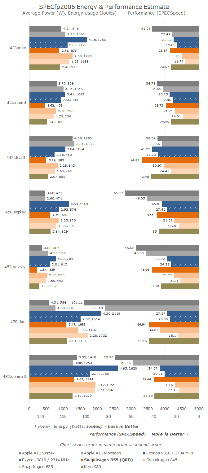
On the SPECfp2006 results, the results can be very clearly categorised into two sets: In one set the Snapdragon 855 clearly showcases a healthy advantage over the Kirin 980, up to very notable 17% and 22% leads in 447.dealII and 453.povray. In the other set, the Snapdragon is again neck-and-neck with the Kirin 980, and these happen to again be the workloads that are most memory sensitive in the FP suite.

Overall, the Snapdragon 855’s CPU performance does not disappoint. Performance on average is ahead of the Kirin 980, although not by much. Here both chipsets are most of the time neck-and-neck, and it will mostly depend on the workload which of the two will take the lead.
More important than performance, the efficiency of the Snapdragon 855 is top-notch, exceeding what I had expected from the higher clock implementation of the chip. There is still a degree of uncertainty over the power numbers on the QRD platform, but if these figures are representative of commercial devices, then 2019’s flagship will see excellent battery life.
Inference Performance: Good, But Missing Tensor APIs
Beyond CPU and GPU, the one aspect of the Snapdragon 855 that Qualcomm made a lot of noise about is the new Hexagon 690 accelerator block.
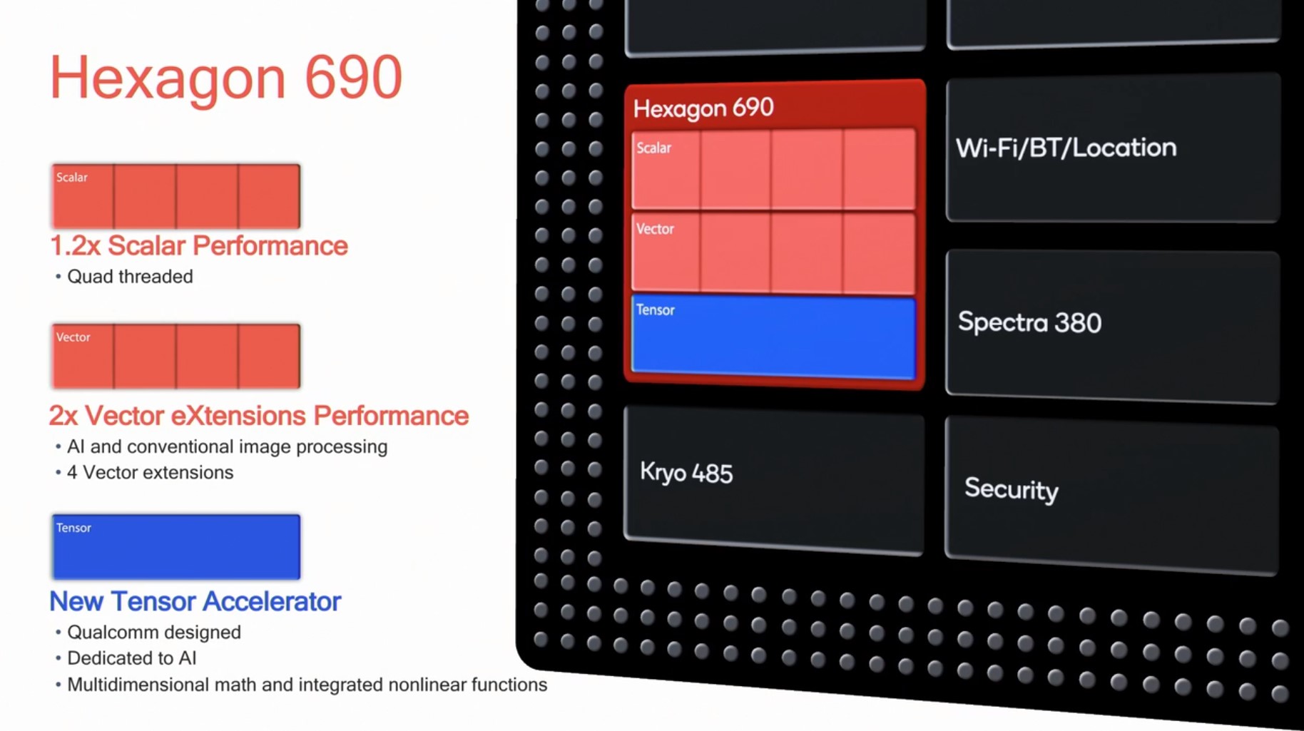
The new unit doubles its vector pipelines, essentially doubling performance for traditional image processing tasks as well as machine inferencing workloads. Most importantly, Qualcomm now includes a dedicated “Tensor Accelerator” block which promises to even better offload inferencing tasks.
I’ve queried Qualcomm about the new Tensor Accelerator, and got some interesting answers. First of all- Qualcomm isn’t willing to disclose more about the performance of this IP block; the company had advertised a total of “7 TOPS” computing power on the part of the platform, but they would not dissect this figure and attribute it individually to each IP block.
What was actually most surprising however was the API situation for the new Tensor accelerator. Unfortunately, the block will not be exposed to the NNAPI until sometime later in the year for Android Q, and for the time being the accelerator is only exposed via in-house frameworks. What this means is that none of our very limited set of “AI” benchmarks is able to actually test the Tensor block, and most of what we’re going to see in terms of results are merely improvements on the side of the Hexagon’s vector cores.
Inference Performance
First off, we start off with “AiBenchmark” – we first starred the new workload in our Mate 20 review, to quote myself:
“AI-Benchmark” is a new tool developed by Andrey Ignatov from the Computer Vision Lab at ETH Zürich in Switzerland. The new benchmark application, is as far as I’m aware, one of the first to make extensive use of Android’s new NNAPI, rather than relying on each SoC vendor’s own SDK tools and APIs. This is an important distinction to AIMark, as AI-Benchmark should be better able to accurately represent the resulting NN performance as expected from an application which uses the NNAPI.
Andrey extensive documents the workloads such as the NN models used as well as what their function is, and has also published a paper on his methods and findings.
One thing to keep in mind, is that the NNAPI isn’t just some universal translation layer that is able to magically run a neural network model on an NPU, but the API as well as the SoC vendor’s underlying driver must be able to support the exposed functions and be able to run this on the IP block. The distinction here lies between models which use features that are to date not yet supported by the NNAPI, and thus have to fall back to a CPU implementation, and models which can be hardware accelerated and operate on quantized INT8 or FP16 data. There’s also models relying on FP32 data, and here again depending on the underlying driver this can be either run on the CPU or for example on the GPU.
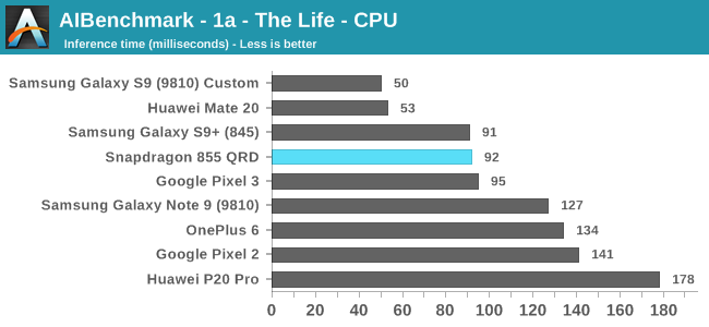
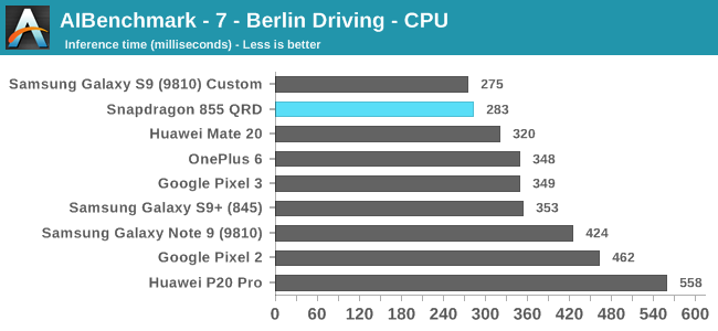
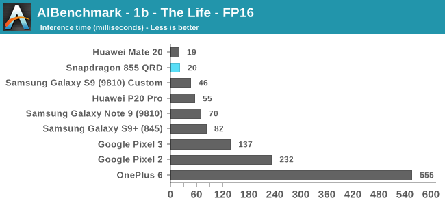
In the first set of workloads which I’ve categorised by being run on the CPU, we see the Snapdragon 855 perform well, although it’s not exactly extraordinary. Performance here is much more impacted by the scheduler of the system and exactly how fast the CPU is allowed to get to its maximum operating performance point, as the workload is of a short burst nature.
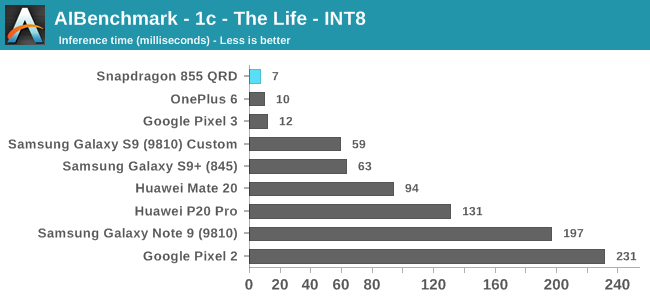
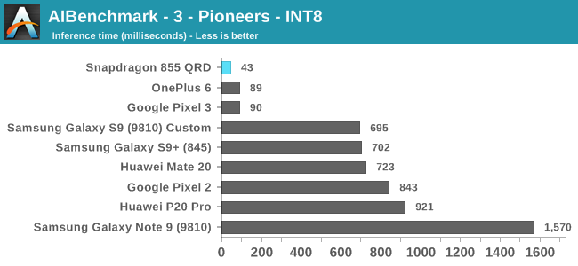
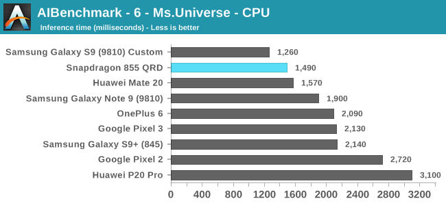
Moving onto the 8-bit integer quantised models, these are for most devices hardware accelerated. The Snapdragon 855’s performance here is leading in all benchmarks. In the Pioneers benchmark we more clearly see the doubling of the performance of the HVX units as the new hardware posts inference times little under half the time of the Snapdragon 845.
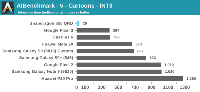
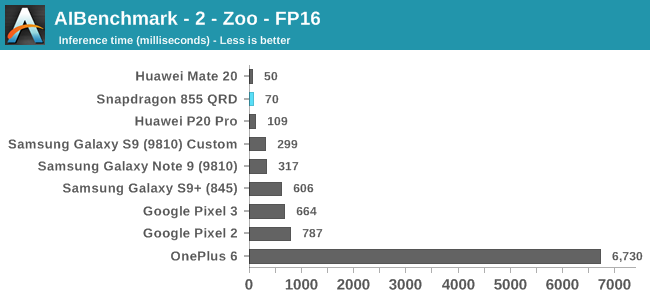
The Cartoons benchmark here is interesting as it showcases the API and driver aspect of NNAPI benchmarks: The Snapdragon 855 here seems to have massively better acceleration compared to its predecessors and competing devices. It might be that Qualcomm has notably improved its drivers here and is much better able to take advantage of the hardware, compared to the past chipset.
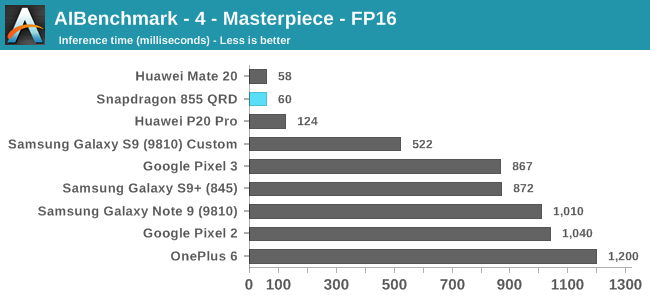
The FP16 workloads finally see some competition for Qualcomm as the Kirin’s NPU exposes support for its hardware here. Qualcomm should be running these workloads on the GPU, and here we see massive gains as the new platform’s NNAPI capability is much more mature.
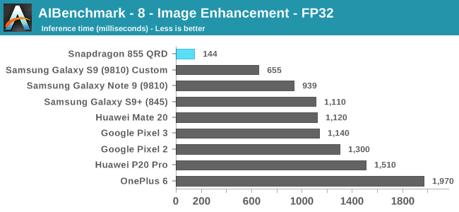
The FP32 workload sees a similar improvement for the Snapdragon 855; here Qualcomm finally is able to take full advantage of GPU acceleration which gives the new chipset a considerable lead.
AIMark
Alongside AIBenchmark, it still might be useful to have comparisons with AIMark. This benchmark rather than using NNAPI, uses Qualcomm’s SNPE framework for acceleration. Also this gives us a rare comparison against Apple’s iPhones where the benchmark makes use of CoreML for acceleration.
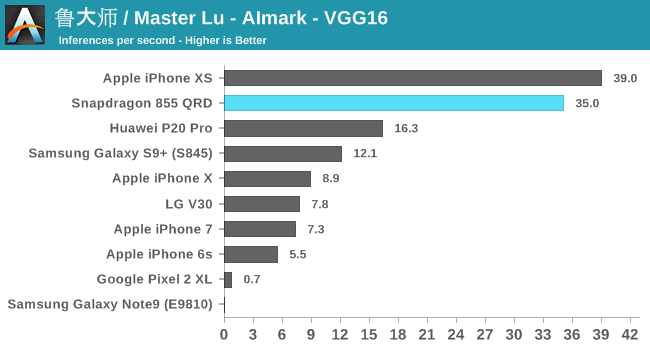
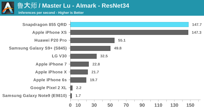
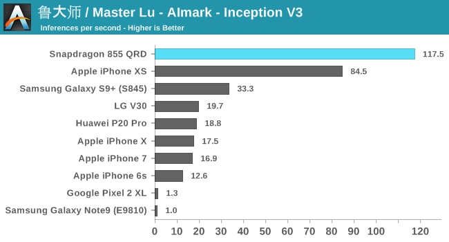
Overall, the Snapdragon 855 is able to post 2.5-3x performance boosts over the Snapdragon 845.
At the event, Qualcomm also showcased an in-house benchmark running InceptionV3 which was accelerated by both the HVX units as well as the new Tensor block. Here the phone was able to achieve 148 inferences/s – which although maybe apples to oranges, represents a 26% boost compared to the same model run in AIMark.
Overall, even though the Tensor accelerator wasn’t directly tested in today’s benchmark results, the Snapdragon 855’s inference performance is outstanding due to the overall much improved driver stack as well as the doubling of the Hexagon’s vector execution units. It will be interesting to see what vendors do with this performance and we should definitely see some exciting camera applications in the future.
System Performance - Slightly Underwhelming?
While synthetic steady state workloads are one thing, real-world workloads are more transactional and their performance is determined not just by hardware, but as well by software. Here things like the CPU scheduler and OS APIs can have a big effect on the resulting perceived performance of a device.
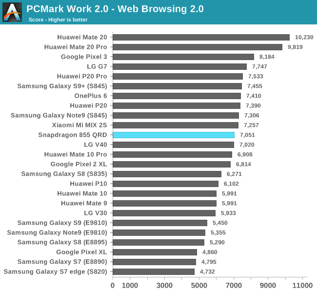
Starting off with PCMark’s Web Browsing 2.0 test, the Snapdragon 855 goes off to a bad start. Here for some reason the S855 QRD wasn’t able to distinguish itself from the lower end of Snapdragon 845 devices – here we had expected the phone to perform and compete similarly to the Kirin 980 in the Mate 20’s.
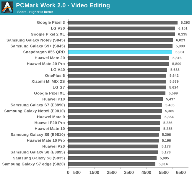
The video editing score is again also quite mediocre, but again the reason for this is that this test has largely reached a performance plateau where most of today’s devices no longer really showcase meaningful differences between each other.
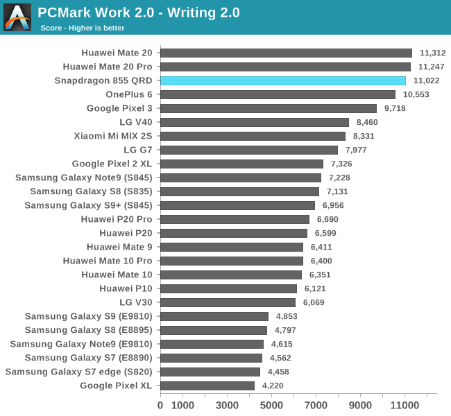
The writing sub-test is among one of the most important in PCMark, and luckily here the Snapdragon 855 QRD performed as expected as it’s within range of the Mate 20’s.
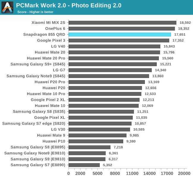
The photo editing sub-test is characterised by shorter heavy RenderScript workload bursts. The QRD performs well, although it’s within the results of the top Snapdragon 845 devices.
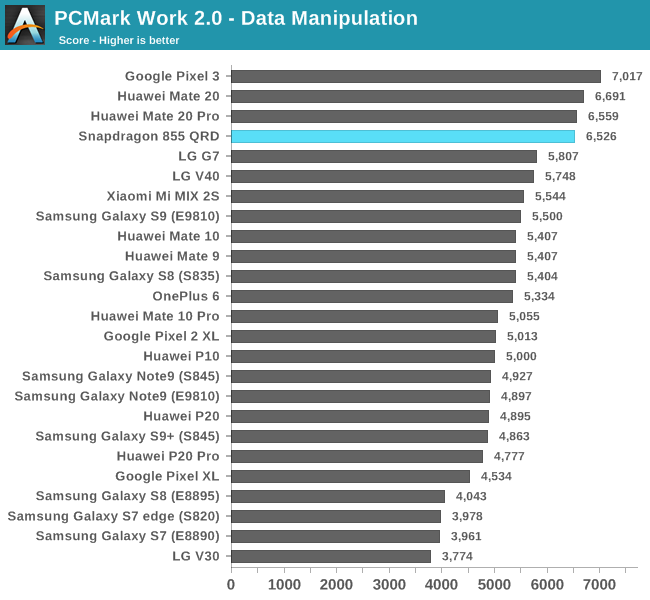
Finally in the data manipulation result which is more single-thread bound, we see the Snapdragon 855 perform well, but still remains neck-and-neck with the Kirin 980 devices as well as behind the Pixel 3’s very aggressive scheduler implementation.
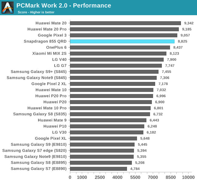
Overall, the Snapdragon 855 QRD in PCMark ended up among the top scorers, however I found the result to be a bit disappointing as it doesn’t appear to achieve a higher ranking than the Pixel 3, and Huawei’s Kirin 980 Mate 20’s are also ahead.
I’ve discussed the results with Qualcomm, and they were surprised to see the numbers end up like this. They stated that it’s something they will look into, and stated that it’s possible that the scheduler and software stack on commercial devices might improve performance. Something to be revisited once we get our hands on the first phones.
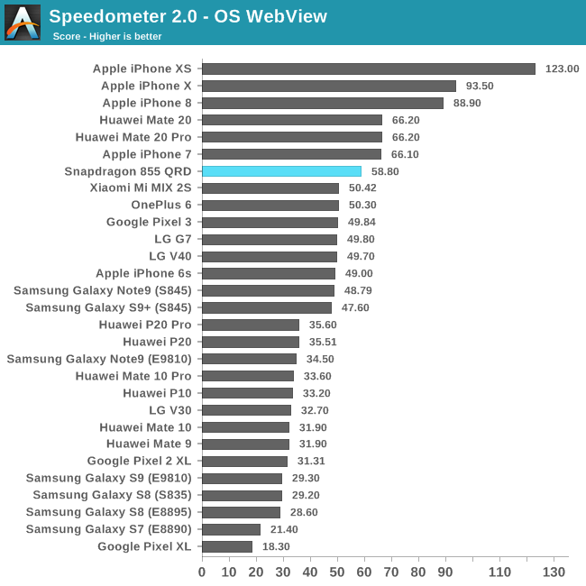
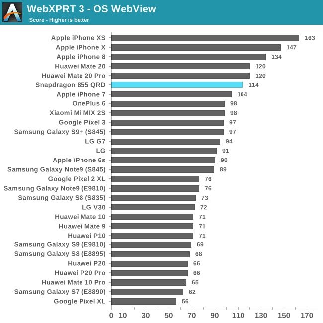
The web-based benchmarks such as Speedometer 2.0 and WebXPRT 3 showcase similar relatively muted results. Here I had expected Qualcomm to perform really well given the scheduler performance showcase of the Snapdragon 845. The results of the Snapdragon 855 are quite meagre, especially in a steady-state throughput workload such as Speedometer 2.0. Here the Snapdragon 855 only manages to showcase a ~17% improvement over the last generation, and also lags behind the Kirin 980 by some notable amount.
Performance Scaling Ramp Test
One of the newer kind of tests I introduced last year and has used in our review of the Apple iPhone XS is the scaling ramp test – here showcasing the improved DVFS responsivity of iOS12 across several generations of iPhones.
I’ve quickly ran this on the S855 QRD to be able to get a sense of the scheduler and DVFS mechanism:
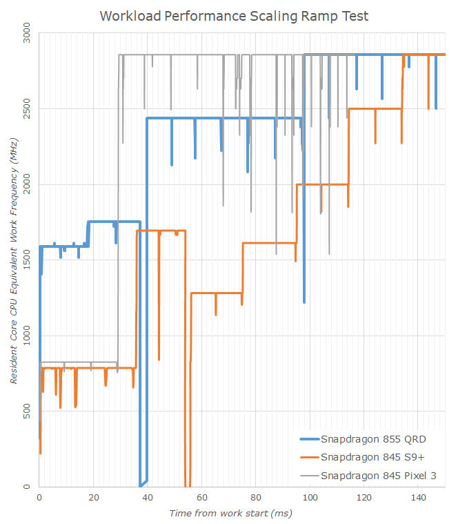
Here we see the Snapdragon 855 QRD being able to scale from a sleeping idle workload state to its maximum performance state in around 100ms. To compare this, I also showcase the scaling behaviour of the S845 in both the S9+ as well as the Pixel 3. The difference between the Pixel 3’s aggressive boost behaviour and the S9’s more step-wise frequency scaling showcases the best visual representation of the perceived responsiveness difference between the two devices.
The Snapdragon 855 here falls somewhere in-between both. It’s to be noted that the workload does get boosted to an “efficient” big core at 2.45GHz in around 40ms which is a very fast scaling behaviour.
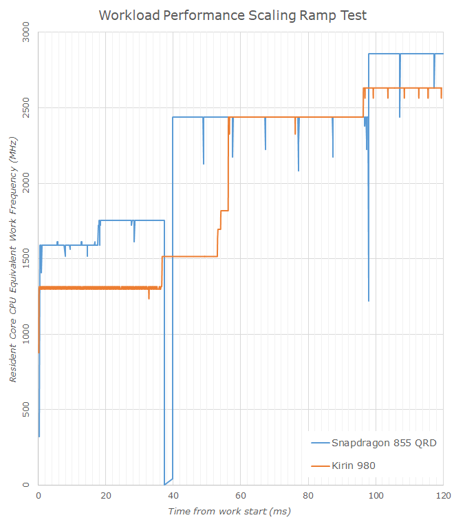
Comparing the Snapdragon 855 against the Kirin 980, we see that the Snapdragon isn’t any slower in reaching the maximum performance states. What is odd in these results is that the workload sees a significant pause of ~2.4ms when migrating over from the little cores, something that seems to affect only devices with Qualcomm’s custom scheduler. It’s an interesting find that I’ll have to investigate more.
Overall, real-world performance of the Snapdragon 855 is a bit lower than I had expected it to be. I’m not exactly sure what the cause here is; on the scheduler side we’ve verified that the workload doesn’t inherently scale slower than the Kirin 980. The only other explanation I could see is that we might be seeing some disadvantage of the smaller L3 cache or even the higher DRAM latency.
As we’ve seen in past Snapdragon performance previews, final commercial device performance is subject to change, and it’s possible the performance situation will be more tuned in actual shipping phones.
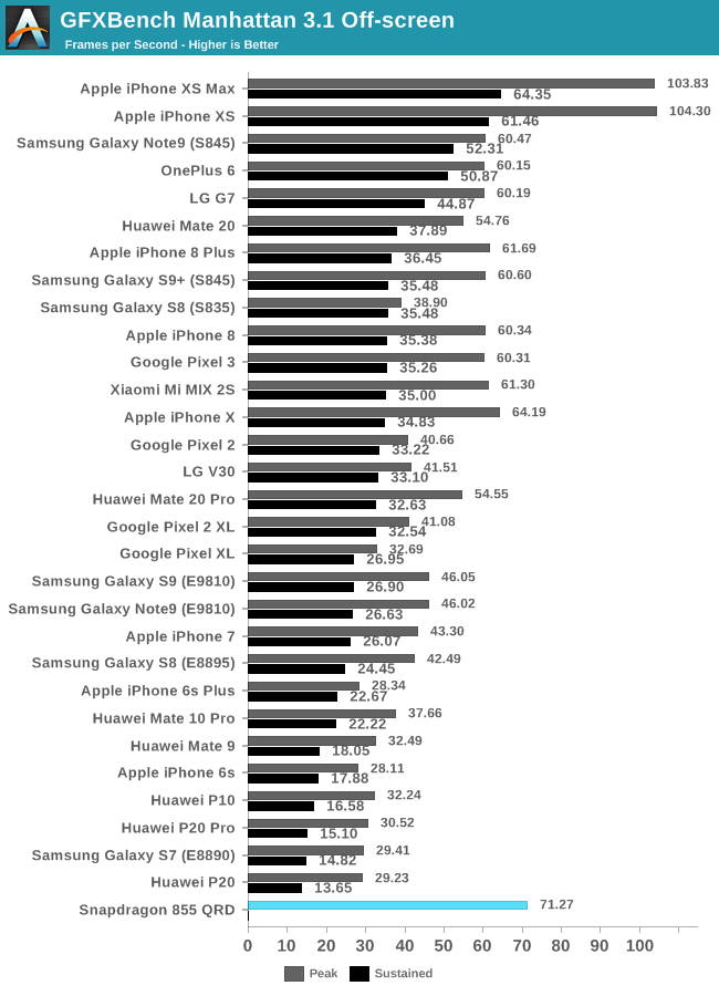
GPU Performance & Power
GPU performance of the new Adreno 640 in the Snapdrago 855 is interesting: The company’s performance claims were relatively conservative as they showcased that the new unit would perform only 20% better than its predecessor. This is a relatively low figure given that Qualcomm also advertises that the new GPU sees a 50% increase in ALU configuration, as well as of course coming on a new 7nm process which should give the SoC a lot of new headroom.
Before discussing the implications in more detail, let’s see the performance numbers in the new GFXBench Aztec benchmarks.
As a reminder, we were only able to test the peak performance of the phone as we didn’t have time for a more thorough sustained performance investigation.
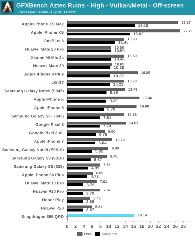
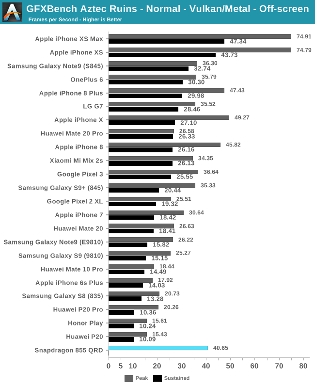
Both Aztec High and Normal results fall pretty much in line with Qualcomm’s advertised 20% improvement over the Snapdragon 845. Here the new chipset falls behind Apple’s A11 and A12 chips – although power consumption at peak levels is very different as we’ll see in just a bit.
| GFXBench Manhattan 3.1 Offscreen Power Efficiency (System Active Power) |
||||
| Mfc. Process | FPS | Avg. Power (W) |
Perf/W Efficiency |
|
| iPhone XS (A12) Warm | 7FF | 76.51 | 3.79 | 20.18 fps/W |
| iPhone XS (A12) Cold / Peak | 7FF | 103.83 | 5.98 | 17.36 fps/W |
| Snapdragon 855 QRD | 7FF | 71.27 | 4.44 | 16.05 fps/W |
| Galaxy S9+ (Snapdragon 845) | 10LPP | 61.16 | 5.01 | 11.99 fps/W |
| Huawei Mate 20 Pro (Kirin 980) | 7FF | 54.54 | 4.57 | 11.93 fps/W |
| Galaxy S9 (Exynos 9810) | 10LPP | 46.04 | 4.08 | 11.28 fps/W |
| Galaxy S8 (Snapdragon 835) | 10LPE | 38.90 | 3.79 | 10.26 fps/W |
| LeEco Le Pro3 (Snapdragon 821) | 14LPP | 33.04 | 4.18 | 7.90 fps/W |
| Galaxy S7 (Snapdragon 820) | 14LPP | 30.98 | 3.98 | 7.78 fps/W |
| Huawei Mate 10 (Kirin 970) | 10FF | 37.66 | 6.33 | 5.94 fps/W |
| Galaxy S8 (Exynos 8895) | 10LPE | 42.49 | 7.35 | 5.78 fps/W |
| Galaxy S7 (Exynos 8890) | 14LPP | 29.41 | 5.95 | 4.94 fps/W |
| Meizu PRO 5 (Exynos 7420) | 14LPE | 14.45 | 3.47 | 4.16 fps/W |
| Nexus 6P (Snapdragon 810 v2.1) | 20Soc | 21.94 | 5.44 | 4.03 fps/W |
| Huawei Mate 8 (Kirin 950) | 16FF+ | 10.37 | 2.75 | 3.77 fps/W |
| Huawei Mate 9 (Kirin 960) | 16FFC | 32.49 | 8.63 | 3.77 fps/W |
| Huawei P9 (Kirin 955) | 16FF+ | 10.59 | 2.98 | 3.55 fps/W |
Switching over to the power efficiency table in 3D workloads, we see Qualcomm take the lead in terms of power efficiency at peak performance, only trailing behind Apple's newest A12. What is most interesting is the fact that the Snapdragon 855’s overall power consumption has gone down compared to the Snapdragon 845 – now at around 4.4W versus the 5W commonly measured in S845 phones.
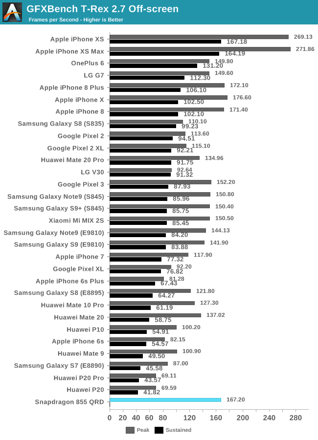
T-Rex’s performance gains are more limited because the test is more pixel and fill-rate bound. Here Qualcomm made a comment about benchmarks reaching very high framerates as they become increasingly CPU bound, but I’m not sure if that’s actually a problem yet as GFXBench has been traditionally very CPU light.
| GFXBench T-Rex Offscreen Power Efficiency (System Active Power) |
||||
| Mfc. Process | FPS | Avg. Power (W) |
Perf/W Efficiency |
|
| iPhone XS (A12) Warm | 7FF | 197.80 | 3.95 | 50.07 fps/W |
| iPhone XS (A12) Cold / Peak | 7FF | 271.86 | 6.10 | 44.56 fps/W |
| Snapdragon 855 QRD | 7FF | 167.19 | 3.83 | 43.65 fps/W |
| Galaxy S9+ (Snapdragon 845) | 10LPP | 150.40 | 4.42 | 34.00 fps/W |
| Galaxy S9 (Exynos 9810) | 10LPP | 141.91 | 4.34 | 32.67 fps/W |
| Galaxy S8 (Snapdragon 835) | 10LPE | 108.20 | 3.45 | 31.31 fps/W |
| Huawei Mate 20 Pro (Kirin 980) | 7FF | 135.75 | 4.64 | 29.25 fps/W |
| LeEco Le Pro3 (Snapdragon 821) | 14LPP | 94.97 | 3.91 | 24.26 fps/W |
| Galaxy S7 (Snapdragon 820) | 14LPP | 90.59 | 4.18 | 21.67 fps/W |
| Galaxy S8 (Exynos 8895) | 10LPE | 121.00 | 5.86 | 20.65 fps/W |
| Galaxy S7 (Exynos 8890) | 14LPP | 87.00 | 4.70 | 18.51 fps/W |
| Huawei Mate 10 (Kirin 970) | 10FF | 127.25 | 7.93 | 16.04 fps/W |
| Meizu PRO 5 (Exynos 7420) | 14LPE | 55.67 | 3.83 | 14.54 fps/W |
| Nexus 6P (Snapdragon 810 v2.1) | 20Soc | 58.97 | 4.70 | 12.54 fps/W |
| Huawei Mate 8 (Kirin 950) | 16FF+ | 41.69 | 3.58 | 11.64 fps/W |
| Huawei P9 (Kirin 955) | 16FF+ | 40.42 | 3.68 | 10.98 fps/W |
| Huawei Mate 9 (Kirin 960) | 16FFC | 99.16 | 9.51 | 10.42 fps/W |
Again switching over to the power and efficiency tables, we see that the Snapdragon 855 is posting a ~30% efficiency boost over the Snapdragon 845, all while slightly improving performance.
Overall, I’m very happy with the initial performance and efficiency results of the Snapdragon 855. The S845 was a bit disappointing in some regards because Qualcomm had opted to achieve the higher performance figures by increasing the peak power requirements compared to exemplary thermal characteristics of the Snapdragon 835. The new chip doesn’t quite return to the low power figures of that generation, however it meets it half-way and does represent a notable improvement over the Snapdragon 845.
Final Thoughts
2018 has been a very successful year for Qualcomm and the Snapdragon 845. The company had provided an extremely solid and well-rounded SoC for device vendors to build their flagship devices on- and by the looks of it the Snapdragon 855 continues this trend.
I’ve been a bit sceptical about the merits of Qualcomm’s 1+3 CPU configuration, however after seeing the preliminary performance and power efficiency figures of the new prime core on the new chipset, I’m not nearly as concerned. We reserve any final verdict for when we will have tested final commercial devices, as that’s where in the end we’ll also see the efficiency effect of the non-prime cores, and how they’ll position themselves against the competition.
Performance wise, the Snapdragon 855 is a bit odd. In steady-state workloads like SPEC the chipset is seemingly performing very well and matches or exceeds the new Kirin 980. Here Qualcomm’s changes to the CPU microarchitecture might even actually be visible in the test results, which is a nice feat. Unfortunately the memory subsystem still seems to include some of DRAM latency regressions that we also saw in the Snapdragon 845, both which are due to Qualcomm’s system level cache.
Real-world performance, while still excellent, doesn’t quite manage to reach my expectations I had for the chipset. Here for whatever reason, the chip’s improvements are not nearly as pronounced as in the more synthetic tests. Again the odd thing is that the Kirin 980 still manages to beat the Snapdragon 855 in near most of these workloads. Qualcomm had reasoned that the microarchitectural changes to the CPU were meant to help web browser performance, yet it’s here where the chip slightly lags behind the competition – I do wonder if this is a case of the CPU again being limited by either Qualcomm’s choice of more conservative caches or due to the latency penalty of the system cache.
Although the performance shown today is exemplary, it still does look maybe a little rough around the edges in some of our system performance tests – here maybe Qualcomm will be able to investigate and further improve things until we actually see commercial devices.
Whether the system performance will be improved in final devices or not, what is clear though is that power efficiency looks outstanding. Qualcomm had me worried as the PR teams had avoided talking about efficiency during the chipset’s launch, but the results today (even if they’ll need to be verified), look very promising and should result in notable battery life improvements in 2019’s devices.
On the GPU side of things, Qualcomm’s more muted performance projections of 20% were because the company has again focused a good part of the process improvements into bringing the overall power back down from the usually higher levels that we saw on the Snapdragon 845.
Overall – the Snapdragon 855 looks to be another extremely well executed SoC from Qualcomm, and I’m looking forward to validating the results and testing out the first commercial devices once they become available.


